Power dividers are probably the most common example of a 3-port device. On the surface, they’re easy to construct with something as simple as a T-junction transmission line functioning as one. However, obtaining good isolation and matching on all ports can be more challenging. A common design to address these concerns is the Wilkinson divider. Despite its simple design, the Wilkinson divider offers excellent performance and can even be iterated in multiple stages for broadband applications.
Specification
There’s not much to say here other than that we’re targeting 1.5GHz as in my other designs. We’d like to see equal power division, i.e. -3dB on both ports, and good isolation between the two ports. It’s worth noting that Wilkinson dividers can be made with arbitrary divisions and ports, but 2-ports with equal split is the most common and is what we’ll be doing here.
Design
Pretty much all we need to do is follow the schematic for a Wilkinson divider (taken from Pozar’s).
\(Z_0 = 50\Omega\) as always, so we have \(\sqrt{2}Z_0 = 70.7\Omega\) and \(2Z_0 = 100\Omega\). Using the line calc in QUCS, we determine the line widths for \(Z_0\) and \(\sqrt{2}Z_0\) to be 2.97mm and 1.54mm, respectively. Similarly, we find \(\lambda/4\) for the \(\sqrt{2}Z_0\) line to be 27.98mm.
The real design challenge is figuring out the best way to realize the transmission line schematic in microstrip. On one hand, we want to keep the split arms far enough apart to avoid coupling. On the other, we want to still be able to keep the lines connecting the resistor short to minimize their transmission line effects. Assessing designs can be really tricky to do without access to EM solvers or more full fledged microwave suites like ADS or Microwave Office. Thankfully, there’s plenty of images and guidance online on microstrip implementations of Wilkinson dividers. I’ve decided to go with the simplest one, which is to just imitate the schematic with a triangular split down the middle.
Simulation
Here’s the schematic laid out in QUCS.
Here’s the simulated results of the power splitting between the two ports.
This looks good. We have a 3dB split at 1.5GHz with only about 0.5dB undesired loss over our operating range.
Next, we have the simulated isolation and input matching.
At 1.5GHz, we have excellent matching and isolation, but this significantly degrades at other frequencies. This is to be expected for a Wilkinson divider though, as they are not broadband devices.
Implementation
This was by far the trickiest circuit to construct, largely due to the angled lines that needed to be cut to a precise width. Unfortunately, I accidentally cut the tape at a few points and had to patch them with solder. This shouldn’t matter too much though. You can also see the SMD resistor I’ve bonded over with copper tape.
First up, we have the \(S_{21}\) and \(S_{31}\) measurements, corresponding to the power division on either port. If nothing else, we’d like to see that our Wilkinson divider indeed behaves as an equal power divider.
\(S_{21}\) measurement:
\(S_{31}\) measurement:
For our \(S_{21}\), we have about -3.8dB at 1.5GHz. And for our \(S_{31}\), we have a slightly better -3.5dB. This isn’t perfect, but it’s still pretty decent. Clearly there’s some loss though. More concerning though is that we have progressively worsening loss and ripple above 2GHz. Below 2GHz, however, there’s little ripple as simulated.
My main guess for the cause of the poor high frequency response is the overall crummy construction job on my part. There’s some jagged cutting where the lines split and between the transitions from \(\sqrt{2}Z_0\) to \(Z_0\) and to the resistor bonding, some of which requiring solder patching due to accidental cuts. Also, I had trouble getting the dimensions down because of the tricky geometry. If you look at my circuit, you can see that the \(\sqrt{2}Z_0\) and \(Z_0\) lines are different widths. I suspect some combination of all of these is troublesome for higher frequencies. The best solution I have would be to just rebuild it more carefully.
The second characteristic we care about is the isolation between the two output ports, or the \(S_{23}\). My measurement for this is below.
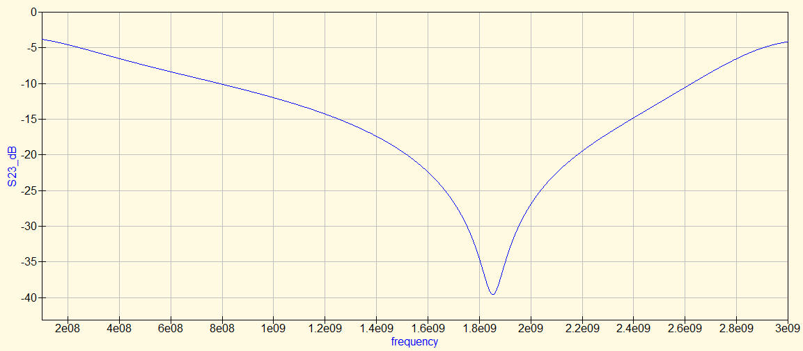
This is odd… we have good isolation, just not where we want it. The null is at ~1.8GHz, not 1.5GHz as we want. At 1.5GHz, we only have about -19dB of isolation, which is alright but we’d certainly like to see better. It’s a bit tricky to diagnose this, but I have a hunch it has to do with the copper tape we used to bond the resistor having undesirable transmission line behavior due to its length.
After fiddling around with QUCS a bit this seems to be the case. I added transmission line element roughly matching my physical circuit to my simulation and was able to recreate what I measured.

This is remarkably close to what I measured. While experimenting with QUCS, I noticed that making the microstrip lines bonding the resistor shorter brought the isolation’s notch frequency down. The takeaway here is that we should opt for a topology which minimizes or outright eliminates, the need for using extra line to bond the isolation resistor. Furthermore, I presume that wire would have too much unwanted inductance to be usable. Many of the Wilkinson dividers I found online seem to have a square/rectangle shape where the two lines separate at a right angle, travel parallel to each other, and then rejoin back at a right angle close enough so that the isolation resistor can be connected directly across. An additional challenge with this is making sure to factor in the bends of the \(\sqrt{2}Z_0\) line when measuring out the \(\lambda/4\) length.
An example I found is shown below. It’s a multi-stage Wilkinson but it still illustrates the point.
If I had more time to rebuild my Wilkinson divider, I would opt for a topology similar to the above but with a single stage of course.